Shaping Tomorrow’s Technologies Through Atomic-Scale Innovation
The rapid growth and widespread availability of data in today’s world is driving demand for faster, more energy-efficient technologies to collect and process vast amounts of information. Meeting this demand requires not just better devices, but fundamentally new materials.
Two-dimensional (2D) materials offer unique advantages including atomic thinness, smooth surfaces without dangling bonds, and diverse physicochemical properties, making them ideal for next-generation applications in computing, communication, energy harvesting, and sensing. Integrating 2D materials with existing silicon circuits also opens new possibilities for enhanced device functionality.
At the Z-SCALE Lab, we focus on atomic-scale innovation in 2D materials to enable breakthroughs across these critical application domains. We tackle key challenges in the 2D materials field through an integrated research framework:
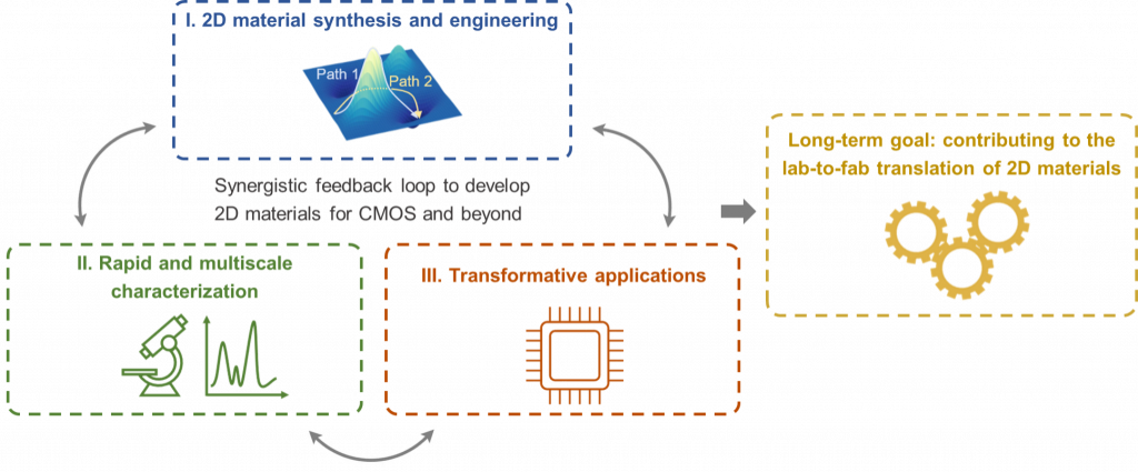
(I) Synthesis and Engineering
We establish new approaches to synthesize large-scale, high-quality 2D materials with precise control over their composition and structure. We also explore atomic engineering and moiré heterostructure construction approaches to tailor their properties and functionalities.
Representative work:
- Hydrogen free-ramping deposition of high-quality 2D semiconductors
- Large-sized in-plane ferroelectric SnSe
- A generalized substitutional doping approach for 2D semiconductors
- A critical review of vapor-phase growth of 2D chalcogenides
(II) Characterization
We develop multiscale and high-throughput characterization strategies to understand how the structure of 2D materials influences their performance. These tools accelerate material discovery and technological advancement by revealing structure-property-function relationships not only at the atomic scale, but also at the device level.
Representative work:
- Cross-correlated tip-enhanced Raman spectroscopy and atomic force microscopy of 2D Janus materials
- Uncovering how edge termination influences dopant distribution in 2D materials
- Raman spectroscopy for atomic defect quantification
- Effects of substrate interaction on optical properties of 2D/3D heterostructures
(III) Functionality and Applications
We explore the functional properties of both intrinsic and engineered 2D materials, leveraging their ultrathin form factor, semiconducting behavior, strong light-matter interaction, and broken structural symmetry. We are also interested in the clean, safe, and scalable integration of 2D materials into device architectures. Our current application domains of interest include but are not limited to artificial intelligence (AI), high-performance computing (HPC), and quantum information science (QIS).
Representative work:
- Clean transfer and integration of 2D materials
- Two-terminal charge-based 2D MoS2 memristors
- Perspective on opportunities and challenges of using 2D materials for logic device scaling
By creating a closed loop through these efforts, we aim to contribute to an accelerated transition of 2D materials from the lab to real-world manufacturing (i.e., lab-to-fab), shaping the future of information and communication technologies.